|
|
|
Basics of Electronics
|
Some of the those basics of electronics which I feel an engineer must never forget.
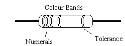
RESISTORS Resistors are devices which limit the flow of
electricity. Resistors are generally made of substances which only
partially conduct electricity such as carbon and some metal oxides. The unit of resistance is "ohm". The
symbol for resistance is the Greek letter W(omega). Resistors are constructed to offer predetermined
resistances. Most common resistors are guaranteed to be within 5% of their
marked value. ('Metal oxide' resistors are rated at their marked value
plus, or minus 1%.) In the early days of electronics, resistors were large enough to have their resistance printed directly onto the body of the device. Modern resistors, however are far too small to allow values to be marked and use a "colour code" consisting of 'bands' painted onto the device. Each colour and its position represents a specific value.
The "tolerance" band indicates the accuracy of the resistor.
Silver
= +/- 10% Resistors with a blue body (metal oxide types) have a tolerance of +/- 1%. The values represented by each colour are:
Black
0 Reading
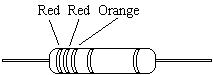
Resistance Values: On 5% resistors (that don't have a blue body) the first two bands represent the first two digits in the number. The third band represents the "multiplier" i.e. the number of zeros to be added after the first two numbers. The value is in 'ohms'. e.g. 1
First two digits : Red, Red - therefore:
2, 2 The value is therefore: 2 2 0 0 0 W, or 2.2 thousand W, or 2.2 kW, or 2.2 kW, or 2k2W. e.g. 2
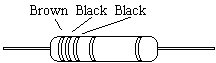
First digit : Brown - therefore:
1 The value is therefore:
10 W,
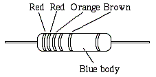
or 10W 1% Tolerance Resistors High accuracy resistors are made using a metal-oxide film, rather than carbon. These resistors have a blue body and four colour bands instead of three. The same colour code system applies, but there are three 'digit' bands and one 'multiplier' band.
First digit : Red - therefore:
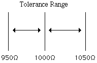
2 The value is therefore: 2230 W, or 2.23kW Standard Resistor Values: With 5%-accurate resistors, there is no point in making values closer than 10% apart. If a 1000ohm resistor can only be guaranteed to be somewhere within the range 950ohm to 1050ohm, there is no point trying to market a 980ohm resistor, for example.
To cater for the 'overlap' in resistor values, a standard 'series of values is used. The
series is called the "E12 series" and was developed in the days
of +/- 10% values. (You can confirm the 'overlap' status of this range for
yourself.) The E12 series is: 1, 1.2, 1.5, 1.8, 2.2, 2.7, 3.3,
3.9, 4.7, 5.6, 6.8, 8.2 in 'tens' this would become: 10, 12, 15, 18, 22, 27, 33, 39,
47, 56, 68, 82 and so on .... When designing projects using 5% tolerance resistors,
the 'nearest' value in the series is chosen. If guaranteed accuracy is required, the 1% 'metal-film' resistors are used. These values are close enough for all but high precision applications. Variable Resistors - Potentiometers: Variable resistors are used in applications such as
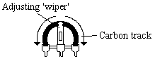
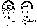
the volume control on a radio receiver and the vertical screen positioning
on a computer monitor. These resistors are constructed with a path of
carbon and a movable 'wiper' which is used to change the length of carbon
path the current flows through.
CAPACITORS In its simplest form, a capacitor consists of an insulator sandwiched between two conductors. The insulator is called a "dielectric" and may consist of almost any insulating material ranging from paper, ceramic, air, oil, plastic and so on. The capacitors used for tuning in radio applications, often have moveable 'plates', but in by far the majority of applications, the positions and sizes of the plates and dielectric are fixed. (Hence the capacitance remains constant.) The unit of capacitance is the Farad (f). (After Faraday) Until very recently, it would be true to say that a 'one-farad' capacitor would be the size of a dinner plate. The 'farad' is a very large unit. The majority of capacitors in general use have values in the rage of micro-farads, nano-farads, or pico-farads!
(One farad
= one million micro-farads Large capacity capacitors are used in domestic appliances such as some video recorders as an emergency memory back-up power supply, rather than using batteries. Typically, these capacitors may have values of five or six farads at 3 volts. The key to understanding the use of capacitors in circuits is that they are basically insulators. If a battery is connected to a capacitor, electrons will flow from the battery onto one of the plates and from the other plate into the battery. This flow of current will continue until the charge on each plate is at its maximum. (As determined by the construction of the capacitor.) For the brief time this process is taking place, there appears to be a complete circuit. If a globe were connected into this circuit, it would glow during the time current was flowing and charging the plates.
Consider then, if alternating current is applied to the capacitor, the plates will be continually charging and discharging as current flows into and out of the plates. A globe connected into the circuit will now remain alight for as long as the varying voltage is applied. A capacitor will therefore conduct changing current, but block Direct Current (DC) (It is important to appreciate that the voltage need not necessarily alternate from positive to negative to be 'passed'; a changing DC current will pass 'through' a capacitor.)
ELECTRICAL CHARACTERISTICS OF CAPACITORS As outlined previously, the main use of capacitors is where the designer wishes to pass changing voltage ( the 'signal') while blocking unwanted DC effects. The choice of capacitor depends upon two factors - the signal voltage and its frequency response. (In some cases, current carrying capacity is also significant.) If the applied voltage exceeds the rating of the capacitor, current may 'punch' through the dielectric from one plate to the other. Maximum voltage rating is usually marked on the capacitor in some way. The size of the plates and the thickness of the dielectric determines the efficiency with which the capacitor will pass a particular signal. A small, thin capacitor is more effective for higher frequency signal than one with large plates and thick dielectric. Physical construction and the type of materials used will also have an effect on the frequency response of capacitors. Once the general type of capacitor has been chosen (refer to the following table), the designer must select the capacitance needed to 'pass' the specific signal. As a general guide, if audio signals are involved (several thousand Hz), typical values would be tens of micro-farads, while radio frequency signals would necessitate the use of pico, or 'nano' values. In reality, consideration must be given to the effects of other components, but the general rule applies.
TYPICAL ELECTRICAL CHARACTERISTICS: Capacitor type Max. voltage Frequency
ceramic
50 volts typical
high (radio) NOTE: This table is meant to
provide a guide only. There
are many
exceptions to the 'voltage' figures
given. In general, a higher voltage rating results in much higher
cost.
CAPACITOR
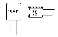
MARKINGS The capacitance of capacitors may be marked in one of several ways. Where there is sufficient room on the body of the device a number and the units will be printed e.g. 100uF 25 VW,
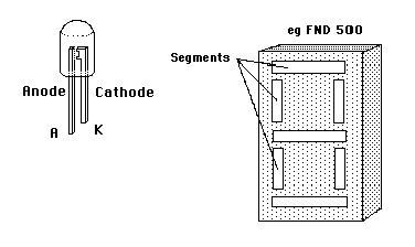
which indicates that this capacitor has a capacitance of 100 micro-farads and a breakdown voltage of 25 volts. (approximately) Smaller capacitors, such as 'greencaps' use a numerical system where the first place represents the first digit, the second place; the second digit and the third place is the number of zeros. (the multiplier) The capacitance so indicated is in picofarads! 104 K = 100,000pF or 0.1uF Colour codes follow a similar pattern to that used for resistors, but they tend to become rather confusing at times. A good set of 'data' sheets should be consulted when decoding is needed. DIODES Diodes are the simplest of solid-state devices. They consist of a piece of P-type material fused to a piece of N-type material. The most common forms of diodes are constructed from Silicon, with Germanium reserved for those special applications where a low forward bias is essential. As outlined later in the section on the "P-N junction", the diode will only conduct in one direction, with electrons flowing from the N-type end to the P-type end. If a voltage is applied which reverse biases the junction, the depletion layer will widen until a point is reached where the voltage exceeds the 'breakdown' voltage of the diode and large currents flow; destroying the device. (One type of diode, the 'zener', actually makes use of breakdown voltage in an interesting way.) There are many different forms of diodes, from simple 'point-contact' signal diodes to multi-coloured light emitting diodes. A few of the more common varieties are discussed below. Signal Diodes Signal diodes are physically small devices usually used where small currents and high frequencies are involved. As will be discussed in the section on 'vari-caps', the size of the junction has an effect on the signal capabilities of the diode. A small junction offers less resistance to high frequencies than does a wide thick junction. As the name implies, these diodes are to be found in the 'signal' section of radios and televisions. ( This role is being phased out by I.C. detectors.) Signal diodes are very small and often glass encapsulated, with a red or black band on one end. (The glass is sometimes painted over to reduce unwanted photo-voltaic effects.
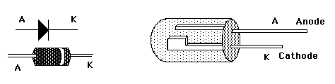
Cathode
K
A Anode Power
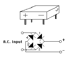
Diodes Where larger currents are involved, a larger junction is needed to dissipate the heat generated. A small junction would be in danger of literally melting with currents in excess of a few hundred milli-amps. Since the power diode has a large junction, it is not suited to high frequency applications. (High frequency, high current diodes are available, but the cost is substantial.) One advantage of the larger junction is its ability to withstand higher voltages without sustaining damage. While a signal diode may only be able to take 30 to 50 volts reverse potential, it is quite common to find power diodes rated up to several thousand volts maximum reverse bias. (Termed "Peak Inverse Voltage", or PIV.) Power diodes are able to pass large loads varying from the 1N400X series rated at 1 amp up to industrial diodes capable of carrying hundreds of amps! These diodes come in a variety of encapsulations, the most common being a black cylinder of plastic about 3mm across with a white band indicating the cathode (negative) end. Large-current devices are often encased in metal to provide efficient heat transfer. It is possible to purchase a 'pack' of four power diodes arranged in a full-wave bridge configuration. (See the section on power supplies.) The physical construction of bridge depends again on the current demand, but all have four leads; two for A.C. input and one each for positive and negative output.
VARICAP DIODE/ VARACTOR DIODE The varicap is a fascinating application of the P-N junction. As discussed later, in the section on the P-N junction, a reverse bias on the 'diode' junction widens the depletion layer. It should remembered that this region is devoid of carriers, or in other words; an insulator. We therefore have an insulator between two conductors, or a CAPACITOR! Varicaps are used in modern 'tuners', such as in televisions and videos. All 'touch-tuning' appliances are based on the varicap principle. A varicap allows the designer to use voltage changes to directly produce a change in capacitance. Light Emitting Diodes Light emitting diodes (LEDs) are among the most widely used of all types of diodes. Colours available range from red, orange, yellow, and the recently developed blue LED Various sizes and intensities are available, with the most common (and cheapest) being the 5mm red led. LEDs are also available in "packages" arranged to produce letters and numerals. The price and availability of these packages depends to a large extent upon current industrial requirements. The once common "FND500" could be obtained for less than a dollar until quite recently. At the moment it costs considerably more, if it can be found at all! (The problem of changing commercial demand for components needs to be kept in mind when choosing student projects.)
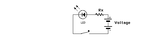
Numerals are produced by arranging LEDs in a seven-segment arrangement as outlined below. I.C.s are available for "driving' displays directly. (The 4026 for example, will take pulses, count them and display the count on a seven-segment display, all for a few dollars!) A LED may be thought of as a 1.5 volt globe for design purposes. If voltages of more than this are involved, a 'dropping' resistor is needed, as indicated below.
Rx = (E - 1.7) x 1000 ÷ I Where E is the input voltage and I is the current in amps. eg: Voltage Rx
6v
330 ohms As with all diodes, orientation is critical. The following diagram should provide a useful guide.
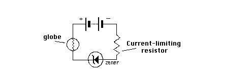
Zener
Diodes If a reverse bias is applied to a diode it will resist conduction until a point is reached where current is forced to flow. This voltage is called the Peak Inverse Voltage, or; breakdown voltage. Under normal circumstances, the diode would be destroyed. It was discovered that precise production techniques could produce a diode with a predetermined 'breakdown' voltage which was less likely to be damaged by 'reverse' current flow. This type of diode is called a "Zener Diode". The result is device which maintains a constant voltage across its ends. Zeners are available in a variety of ratings, the most economical being a one watt version. 'Voltages' usually follow the E12 series, i.e. 1.5, 2.2, 3.3, etc. It must be remembered that Zeners are used in REVERSE mode, i.e. the anode connects to the negative supply.
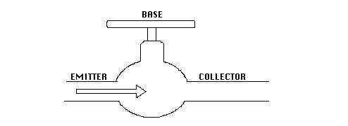
TRANSISTORS - General The transistor may be thought of as an electronic tap, able to control a large flow of electrons with only small variations of the 'spigot'.
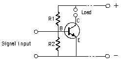
The 'tap' is controlled by varying the voltage between the emitter and base of the transistor. The main 'flow' is a path between the emitter and the collector. As outlined later, in the section on the 'Bi-polar' transistor, in order to turn on the emitter-collector pathway, a forward bias of at least 0.6 volts is needed between the emitter and base. In a PNP type, this means the base bust be at least 0.6 volts 'more negative' than the emitter and in a PNP type, the base must be at least 0.6 volts 'more positive'. The actual base current is chosen in order to provide a 'linear' response to the applied signal. (i.e. the amplified signal is proportional to the changing base current). Biasing Transistors: To keep the transistor operating within this useful range, resistors are used to establish a predetermined potential difference between emitter and base and base and collector. These resistors are called 'bias' resistors. There are a variety of ways to provide the correct 'bias' to a transistor, one of the most common is presented below:
Resistors R1 and R2 form a 'voltage divider' which establishes correct bias and ensures a 'linear' response. A REGULATED POWER SUPPLY The following circuit is presented in order to give some insight into the design of a typical power supply. The most significant feature of this supply is that the collector of the output transistor may be connected directly to the case of the unit, providing a considerable saving by eliminating all heat-sinking. The supply could be expected to deliver several amps continuously.
Circuit
Design and Theory by:
Reg Ion (Technician) The voltage at the emitter of Q1 is set by the zener. (In this case at 6.4 volts.) The base of Q1 is therefore at 5.8 volts. (0.6 volts 'lost' because of the barrier potential across the emitter/base junction.) The ratio of RA and RB is calculated to produce approximately the zener voltage at the bottom of RA. e.g. if the output voltage is 12 volts the ratio required is 5.6 to 6.4. The 'ratio' of RA to RB could therefore be 5.6k to 6.8k (E12 series) The
Regulated Power Supply - HOW IT WORKS: If the output voltage increases, the voltage at the junction of RA and RB also increases. In other words, the voltage at the base of Q1 rises. This tends to turn off Q1 which turns off Q2 and Q3. (Reduces the current, rather than turning them off completely.) The opposite occurs if the voltage tends to drop off. A constant voltage is therefore maintained at the output of the supply. In practice, RA would be adjustable, in order to set the output exactly. RS - provides a 'starting load' for the supply. A voltage must appear at the base of Q1 before the circuit will operate. RS allows current to flow at 'switch on' and to establish the necessary potentials around the circuit. (For a very small load, RS may be reduce in value.) CL - provides improved stabilisation. i.e. ripple is further reduced. RG and Globe - prevents the generation of excessive voltage at the output when loads are very small. If Q3 switches off under light loading, the current flowing through RS could allow the output to rise to the voltage at the output of C1 and C2. The small current flowing through the globe prevents this from happening. (RS is chosen to limit the current through the globe to 'safe' levels.) RZ - limits the current passing through the zener. C1 - provides a degree of 'smoothing'- about 10,000uf total is adequate. D1 - D4 - rectify the transformer output. TR - mains transformer with about 20 volts output.
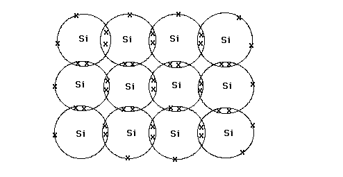
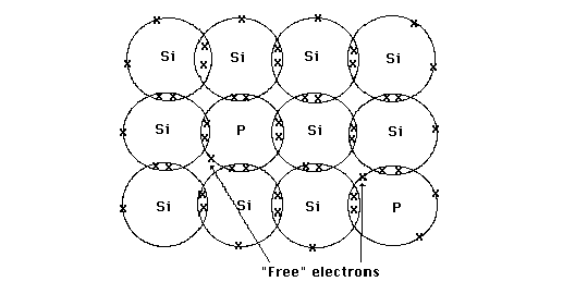
CHOOSING THE TRANSISTORS: The choice of Q1, Q2 and Q3 is an interesting exercise in itself. You must work 'backwards' from Q3. The most economical choice for Q3 would be a 2N3055. This transistor can pass up to 15 amps and is easily bolted directly to the case. (Without the use of an insulating washer!) The required output voltage is also well within the specifications for this transistor. Having selected Q3, we must determine its optimum base current . (Data tables need to be consulted.) Q2 is selected according to its ability to deliver this base current to Q3, keeping in mind the current available from Q1 and the gain of Q2. Q1 is then selected according to the base current needed by Q2, keeping in mind the gain of Q1 and current available from RA. This may seem complex at first, but in reality it is very simple. The complication arises because we must consider the current needed by the following transistor, while working out the base current and gain of the preceding transistor. Say for example that Q3 requires a base current of 100mA. Q2 must deliver this current having 'amplified' its own base current. We therefore need to know the gain of Q2 and the current available from Q1. The base current of Q1 is determined by the value of RA and RB. A small signal transistor such as a BC558 has a gain of several hundred, so even a few milliamps at its base will provide tens of milliamps at the base of Q2. It is therefore not all that important to know the exact base current of Q1, as long as a high gain transistor is used. Perhaps more important is the choice of Q2. This transistor must be able to provide sufficient gain and power handling to 'amplify' tens of milliamps into the hundred, or so needed by Q3. A typical choice would be a BD139. The preceding was presented for two reasons. Firstly to provide an insight into the theory of power supplies and secondly (and most importantly) to try to show that electronic design is demanding, but by no means impossible. With a good set of data tables and an understanding of basic transistor theory such as 'gain' and 'base current' anyone could select suitable replacement for Q1, Q2 and Q3. (Give it a go!) SOLID STATE THEORY P-type and N-type Material: Electricity travels through substances when electrons move from place to place within the substance. Elements which have outer electrons held less tightly than inner ones may have a number of "free electrons" which are able to move around and take part in this process. Substances such as Silicon have some "free electrons", but not as many as a substance such as copper. By adding certain 'impurities' to crystals of silicon, or Germanium, more free electrons (Carriers) may be liberated. The diagram below represents the structure of a 'normal' pure crystals of Silicon. (Only outermost electron are shown.) Notice that each atom shares eight electrons. Under these circumstances, all electrons are bound strongly to the nucleus, leaving few "free electrons" in the crystal.
If a few atoms of phosphorus are added to the crystal, unpaired electrons are now free to move within the crystal structure. The process of adding selected 'impurities' to Silicon is termed "Doping".
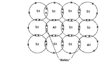
f atoms of Aluminium are diffused into a Silicon crystal, the following arrangement will occur.
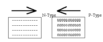
In this case, spaces, or 'holes' exist where electrons could exist. Electrons can move from one end of the crystal to the other by 'jumping' from hole to hole. (It could in fact be imagined that the 'hole' is moving in the opposite direction!) As the above two examples illustrate, conduction through 'doped' Silicon differs. In one case, conduction is by electron flow and the other by 'hole' flow. (This is not just a case of semantics, there are measurable differences between the two!) Materials which conduct by electron movements are called: N-type. Materials which conduct by 'hole' movement are called: P-type THE
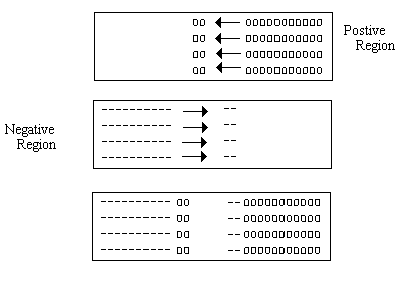
P-N JUNCTION When a piece of P-type and N-type material are fused (melted) together an interesting phenomenon occurs. The following diagrams show diagrammatically what happens to carriers within the resulting fused mass.
(Only one type of carrier at a time will be shown in the following diagrams.) On fusing, carriers 'migrate' into the opposite region because of attraction between opposite charges.
This process continues until the number of carriers which have crossed the 'junction' have a large enough charge to repel any others and prevent the others from crossing. A "barrier potential" is set up within the device, preventing carriers from crossing the barrier. The region between is free of carriers and is termed the "depletion layer" The voltage needed to overcome this 'barrier potential' and allow carriers to move across the junction is dependent upon the conductor material. For Silicon it is 0.6 volts and for Germanium it is only 0.2 volts. NOTE:
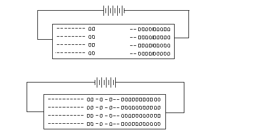
If a reverse potential is applied to the junction ('reverse bias')
the depletion layer becomes even wider, making it even more difficult for
conduction through the device. REVERSE BIAS
FORWARD BIAS
MAJORITY and MINORITY CARRIERS: The preceding discussion has assumed that the conducting material is either 'pure' N-type, or 'pure' P-type. In reality, any conductor will have some impurities. In P-type material, the majority of carriers are 'holes' and only some current flow is due to electrons. ("Electrons" in this sense as discussed previously - obviously all flow is due to electrons.) In P-type material then; 'holes' are majority carriers and 'electrons' are minority carriers. Similarly, in N-type; 'electrons' are majority carriers and 'holes' are minority carriers. The small 'reverse' current across forward biased junctions is due to the flow of minority carriers, which 'see' the junction as forward biased. Flow due to this phenomenon is termed 'leakage current'. This concept of minority flow across a 'reverse biased' junction is key to understanding the operation of most semiconductor devices.
THE
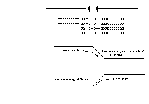
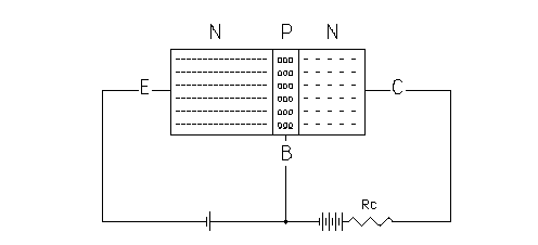
BI-POLAR TRANSISTOR An examination of how the Bi-Polar transistor works should provide an insight into the physics of similar multi-junction devices.... A bi-polar transistor consists of three 'doped' pieces of semiconductor material fused to produce a device with two 'junctions', each with characteristics similar to the basic P-N junction discussed in the previous section. The ease with which the carriers can move across a junction may be represented by an 'energy level diagram'. Consider firstly, energy levels across the basic 'diode' junction.
As can be seen from the diagrams; when forward biased, majority carriers from each side will readily flow 'downhill' to a lower energy state across the junction. Minority carriers, on the other hand see the junction as a 'hill' and will not readily flow to the higher energy state. The small current which does flow is called: 'leakage current'. When three pieces of semiconductor material are fused together, the situation becomes slightly more complex, but the same basic 'diode' principles apply. The bi-polar transistor is constructed with a heavily doped emitter, a very thin base and a lightly doped collector.
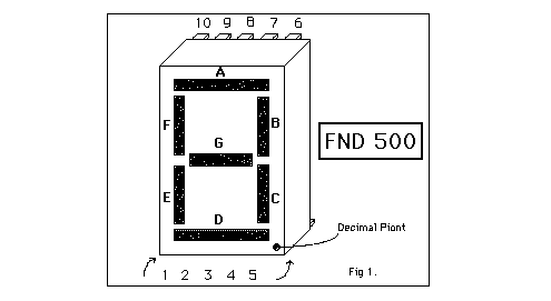
Electrons flow from the emitter to the base region, but since the base is so thin, most diffuse into the collector. While this region is reverse biased for holes, it is forward biased for the electrons which have just arrived. The light doping of the collector prevents too high a degree of repulsion between the electrons in the collector and those which arrive from the emitter. (via the base) The small base current 'removes' any electrons in the base region which would otherwise tend to block the flow of current from the emitter. As the collector-base junction is reverse biased (for majority carriers), the collector supply voltage may be considerably larger than the base-emitter junction voltage. This allows a large 'load' resistor to be connected in series with the collector as shown. (Rc above) In other words, the low resistance of the base-emitter junction has been transferred to a higher resistance in the collector circuit. (ie "Transistor") The same principles apply for PNP transistors, but the charges on the majority and minority carriers are opposite. Seven Segment Display A "seven segment display" consists of seven separate segments, made up of LEDs, Fluorescent tubes, or magnetic panels (on some petrol bowsers) which can be individually activated to display digits. One of the most common electronic versions of such displays is made up of seven rectangular LEDs moulded together into a single digit 'block'. One leg of each individual LED connects to a pin at the rear of the device and the second legs are all connected together as a single "common" pin. Depending upon which arrangement is used, the display is described as "common cathode", or "common anode". The FND 500 is a "common cathode" display.
Pins 3 and 8 are connected to the cathodes of each LED (the negative leg). Either pin may be connected to the negative line. A positive voltage at appropriate pin will light the corresponding LED segment. e.g. ... FND 500 pin configuration
1 -
E
6
-
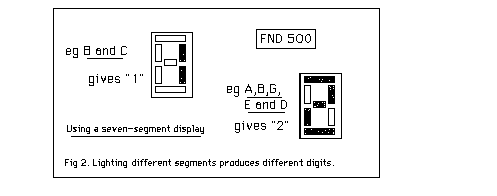
B A special purpose Integrated Circuit (IC) is used to control the display and illuminate the appropriate segments in order to produce the desired digit. e.g. Lighting up segment "B" and "C" produces the numeral "1". Segments "A", "B", "G", "E" and "D" produce "2". Other digits from 0 to 9 are all produced in the same way. (Some displays of this type have a few extra segments which allow letters to be produced as well as numerals.)
The 4511 and 4026 "driver" ICs may be used with the FND 500 to produce the appropriate segment display for each digit required. NOTE: To limit current through the LEDs, a "dropping" resistor may
be inserted between "common"
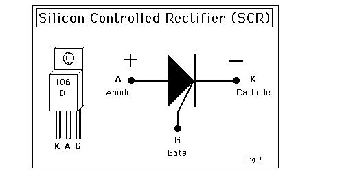
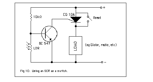
(pins 3, or 8) and the negative line. Silicon Controlled Rectifier (SCR)
The SCR is a high-current, high-voltage solid state switch. A typical SCR, such as the C106D is rated up to 400 volts at 4 amps! Only a few milli-amps between the "Gate" and "Anode" will "trigger" the SCR, which will continue to conduct until the voltage across A-K is removed (or reversed). For low voltages, a "shorting switch" across A-K will stop conduction (ie turn it off!) In the case of an AC supply, this resetting action will occur each time the cycle changes. The SCR will therefore only continue to conduct AC while the Gate current is present. The SCR is very easy to trigger, but usually
requires manual resetting, or complex circuitry to perform an 'electronic'
reset. Typical Application:
The circuit outlined above may be used to control any battery-operated device up to around 30 volts and drawing no more than about one amp. Simply cut the power lead and connect leads to the device so that it becomes the "load" represented above. NOTE: This
circuit must NOT be used on mains-connected devices, or high-current loads
(such as car horns.) It would be safe to use a battery/mains device but
ONLY with the mains disconnected. As a general rule - unless you are sure
- DON'T!! This
article is a original property of Jim Fuller |